

PCB Design with EasyEDA Online Platform: A Complete Guide
Creating a Printed Circuit Board (PCB) is an essential step in turning your electronic project into a compact and portable device. With the right tools and knowledge, designing a PCB becomes easier, ensuring reliable connections and a professional finish. In this blog, we will guide you through the process of designing your own PCB using the EasyEDA online platform. We’ll walk you through the steps involved in designing a simple water level indicator PCB, but the same principles apply to any circuit you want to create.
Why Choose EasyEDA for PCB Design?
EasyEDA is one of the most popular online platforms for PCB design, and for good reason. While it’s not the only tool available, its user-friendly interface, ease of access, and real-time updates make it an excellent choice. Here are some reasons why I prefer EasyEDA:
- No Software Installation: As an online platform, EasyEDA eliminates the need to install any software on your computer. You can access it from any device with an internet connection, and it’s constantly updated with new features and components.
- Cloud-Based Sharing: EasyEDA makes it simple to share your PCB designs with the world. You have the option to keep your designs private or publish them publicly. This flexibility makes it easy to collaborate and learn from others.
- Regular Updates and New Components: The platform offers a wide variety of components and keeps updating its libraries to include new parts regularly.
With these features, EasyEDA simplifies PCB design for both beginners and professionals. Let’s dive into how you can create your first PCB using this powerful tool.
Getting Started: Designing Your First PCB
Before diving into PCB design, you should have a basic understanding of circuit design. It’s always a good idea to test your circuit on a breadboard (zero board) to ensure it works as expected. Once your circuit is confirmed to function properly, you can move forward with the PCB design.
Here’s how to start designing a PCB for a Water Level Indicator project using EasyEDA:
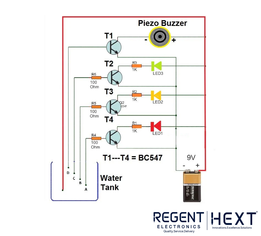
Step 1: Create a Circuit Diagram
Start by creating a schematic for your circuit. This diagram visually represents how the components are connected. Once you’ve made the circuit and tested its functionality, you can move to the next step.
Step 2: Sign Up and Set Up EasyEDA
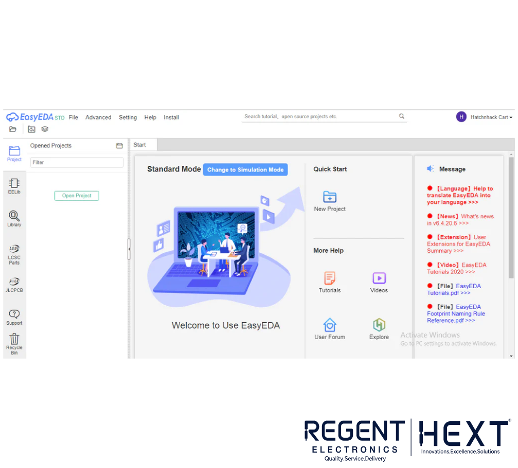
- Visit the EasyEDA website and sign up for a free account.
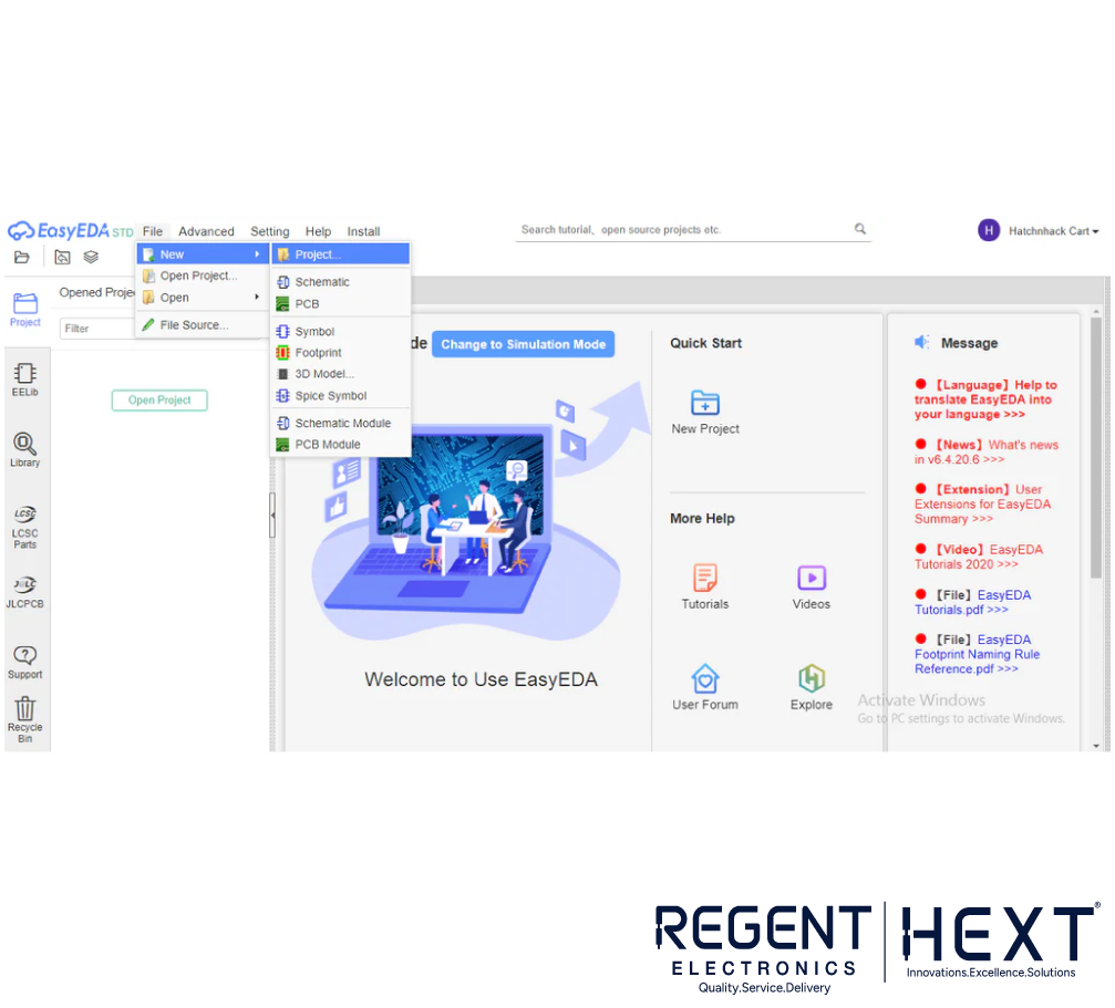
- After logging in, click on File > New > Project to begin a new project.
- Give your project a title, and hit Save.
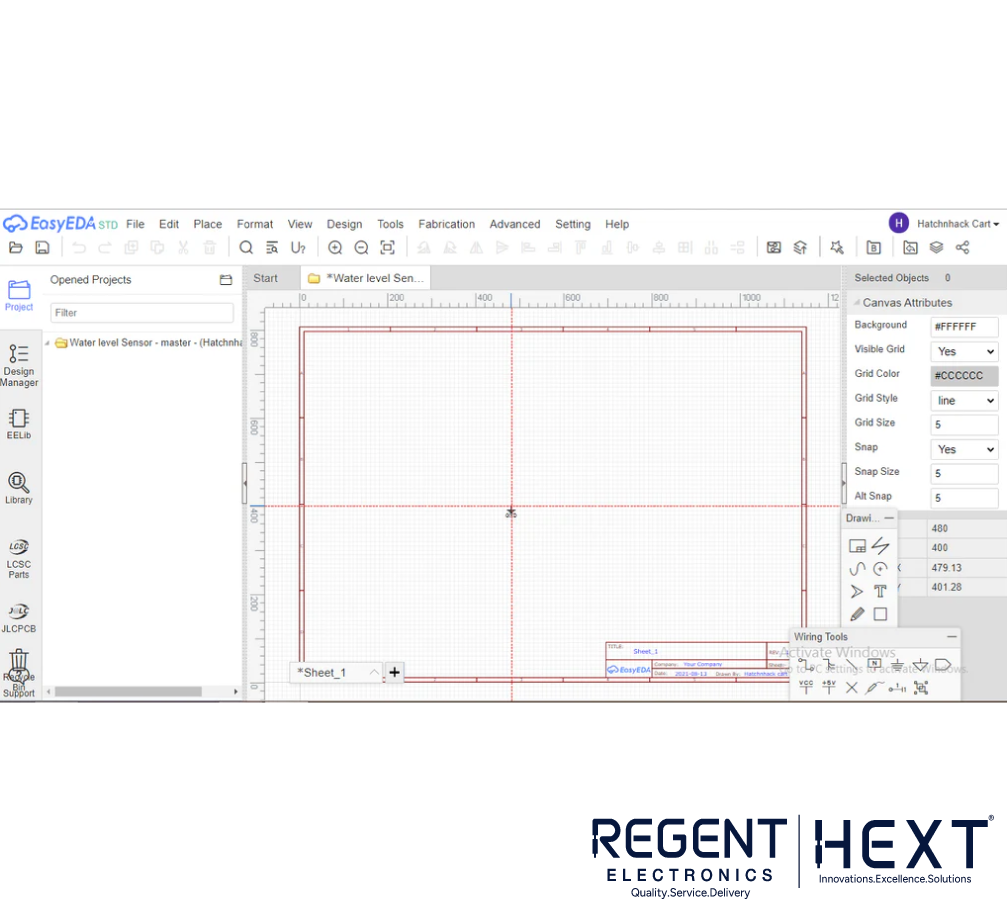
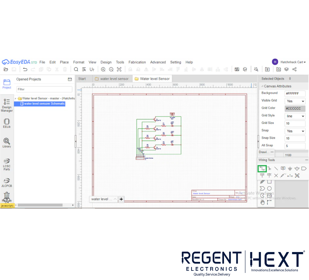
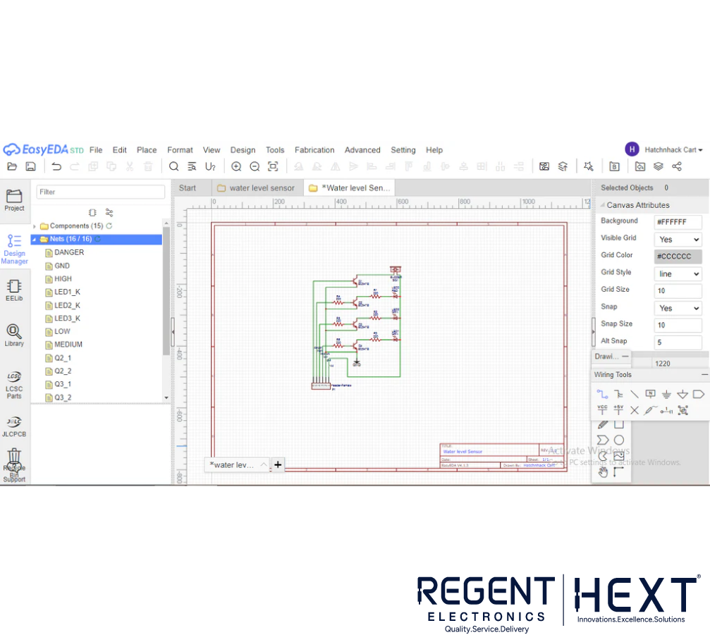
Step 3: Create Your Circuit Schematic
- You will now see a blank design sheet. This is where you will create the schematic of your circuit.
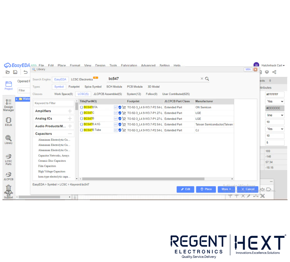
- To add components, click on the Library tab and search for the components you need. You can search by component name or code. Select the most suitable option for your design.
- Use the Wire Tool (found in the toolbox on the right) to connect the components. Additionally, you can use the Ground and VCC options from the same toolbox for power connections.
Step 4: Convert Schematic to PCB Layout
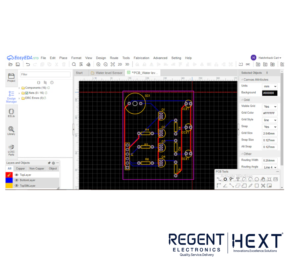
Once the schematic is complete, it’s time to convert it into a PCB layout. To do this:
- Click on the Convert to PCB option from the toolbar at the top.
- A warning will appear asking you to check for any unfinished nets. If you have any unconnected parts, click Yes to connect them.
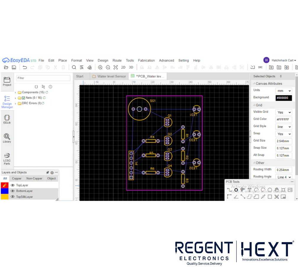
- Click Convert to PCB again, and you’ll be redirected to the PCB layout screen where your schematic will appear as a rough layout outside a rectangular board outline.
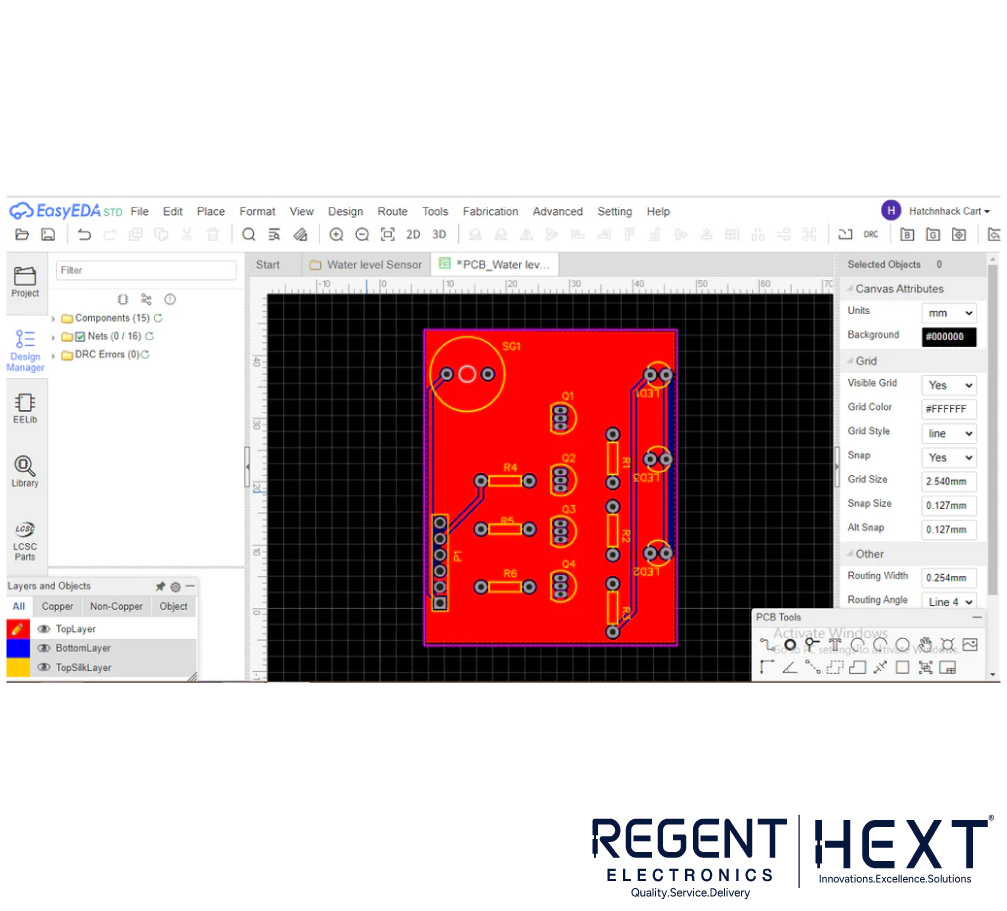
Step 5: Set Up PCB Dimensions and Components
- In the Units Menu, select mm as the unit of measurement.
- Set the PCB Size of your choice and place the components inside the board outline.
Step 6: Set PCB Design Parameters
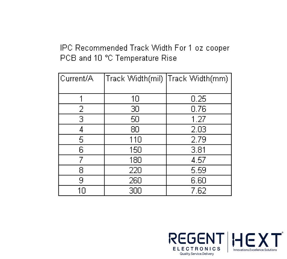
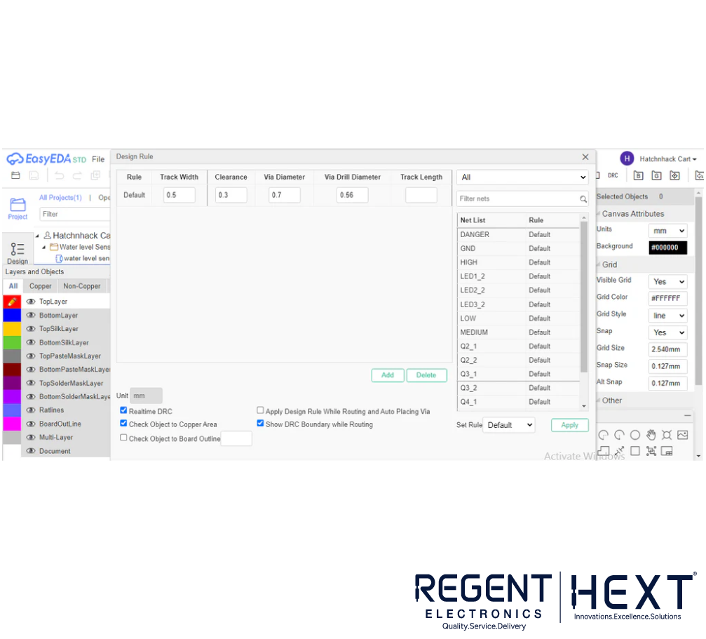

To ensure your PCB is designed for optimal performance, follow these steps:
- Click on Design > Design Rule from the top toolbar.
- In the new window, set the parameters for your PCB. This includes trace width, clearance, and other design rules.
- Once you’ve set the parameters, you’ll see the changes reflected in your PCB layout.
Step 7: Add Ground Plane for Improved Performance
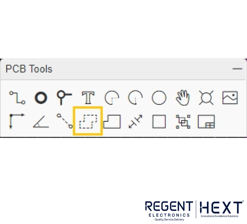
To improve your PCB design, you can add a Ground Plane. This will help with temperature stability and reduce copper waste. Here’s how:
- Select the GND Copper Surface option from the toolbox.
- Draw an inner boundary around your PCB layout and name it GND in the netlist. The ground points will automatically connect to the copper surface.
Step 8: Check for Design Rule Errors
It’s essential to check for any errors in your PCB design. To do this:
- Click on Design > DRC Check (Design Rule Check).
- If there are no errors, congratulations! Your PCB is error-free and ready for manufacturing.
Step 9: View Your PCB in 3D
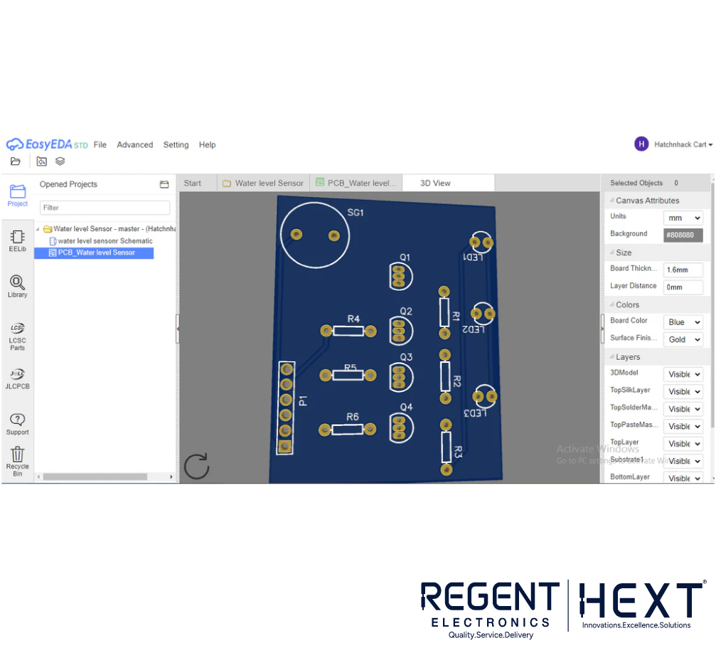
For a more detailed view, you can check your design in 3D. This will give you a realistic look at how your PCB will appear once it’s fabricated.
Conclusion
EasyEDA provides a convenient, user-friendly platform for designing PCBs, from schematic creation to final layout. Whether you’re a beginner or an experienced designer, EasyEDA makes it easy to bring your electronic projects to life. From the water level indicator to more complex circuits, the process is straightforward and accessible.
If you’re looking for high-quality PCBs or need help with your PCB design projects, Regent Electronics offers a wide range of services and components to help bring your designs to reality. Start your PCB design journey today and take advantage of the powerful tools available in EasyEDA!
By following the steps outlined above, you’ll be well on your way to creating your own professional PCBs without the need for expensive software or complex installations. Happy designing!